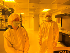
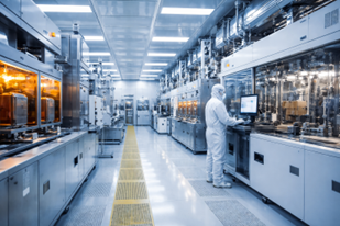
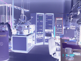
Keck Microfabrication Facility
![]()
History:
Founded in 1994 as one of the first NSF Materials Research Science and Engineering Centers, the Center for Sensor Materials embodies interdisciplinary materials research with emphasis on sensing applications. The CSM shares its four major facilities with campus users and with a national network of 24 MRSEC's, extending its research capabilities throughout academia and the industrial sector.
Under the aegis of the National Science Foundation, the CSM Microfabrication Facility was opened to users in 1996. The original 1200 square foot facility consisted of a Class 1000 cleanroom for photolithography; a room dedicated to electron beam lithography, and an area for sample preparation, metallization, and processing. In 1998, the facility was named the W. M. Keck Microfabrication Facility in recognition of the support of the W. M. Keck Foundation and relocated to the basement level, Room 36, of the old Physics and Astronomy Building at MSU. Recognizing its importance, Michigan State University constructed a new home and upgraded the facility in 2002 in the Biomedical and Physical Science (BPS) Building on the MSU campus.
The Keck Microfabrication Facility (KMF) continues to this day and provides a unique research and training environment on the Michigan State University campus, bring together students, faculty, and industrial scientists. In its current form the ~3000 square foot facility features a Class 100 cleanroom for photoresist preparation and photolithography, three bays for scanning electron microscopy and electron beam lithography, and a vastly increased space for installing new equipment to meet the ever-evolving demands of modern nanofabrication and quantum nanotechnology.
Capabilities:
The Keck Microfabrication facility at MSU provides a unique suite of micro- and nano-fabrication equipment needed for processing and characterizing a variety of devices for quantum information science and computing. This includes a dedicated Plassys electron beam evaporator for making high-coherence Josephson Junction-based superconducting qubits, aluminum and niobium-based high quality factor resonators, and high-impedance microwave devices based on granular aluminum. Furthermore, the facility is equipped with characterization tools for the room temperature testing of qubit junctions. Additionally, the KMF has recently installed a Heidelberg DWL 66+ mask-less UV lithography tool that can be used for creating features down to 600 nm on chips as small as several millimeters on a side to wafers as large as 8 inches in diameter. This tool is particular useful for direct fabrication of structures onto the surface of quantum grade diamond and other insulating materials, where e-beam lithography proves to be cumbersome due to substrate charging. Coupled with these lithography capabilities are pulsed and continuous wave (cw) optically detected magnetic resonance (ODMR) tools for characterizing the coherence of color-center qubits in diamond-based devices.
All of this equipment is available for use by internal and external users, with modest user fees. The Keck facility employs a full-time staff scientist, who trains all new users and maintains the equipment.
The KMF includes the following fabrication equipment:
- Hitachi SU5000 field-emission SEM with NPGS electron beam lithography system
- Heidelberg DWL 66+ (minimum resolution 600 nm)
- Plassys MEB550S electron beam deposition system (dedicated for superconducting qubit fabrication, to be installed September 2026)
- Hitachi S-4700II FESEM
- Scanning Probe Microscope
- Room temperature probe stations for superconducting qubit (Josephson Junction) characterization
- Pulsed and cw ODMR tools for characterizing color-center qubits in diamond.
- X-ray Microanalyzer
- Micro-Raman Spectrograph
- Optical Microscopes
- Optical Imaging System
- High resolution X-ray diffractometer
- Mask Aligner
- Resist Preparation Equipment
- Thin film thermal deposition systems
- O2 Plasma Etcher
- Reactive Ion Etcher with Inductively Coupled Plasma (ICP) option
- Vacuum Oven
- Sputter coater for SEM sample prep.
- Surface Profiler
- Wafer Dicing Saw
The KMF is also connected to a shared user facility, i.e. the MSU Physics and Astronomy Sputtering Facility (SF) that provides users with ultra-high vacuum, dc-magnetron (triode) sputtering systems for the deposition of high-quality thin films of a variety of materials. These include standard superconductors such as niobium as well as high-kinetic inductance materials such as niobium nitride, TiN, and NbTiN for creating high-impedance superconducting resonators used in circuit quantum electrodynamic (cQED) systems with superconducting qubits. Additionally, the sputtering systems can create thin films of rare-earth magnets and piezoelectric insulators (AlN) for integration with hybrid quantum systems-based devices containing superconducting qubits or color-center qubits in diamond. This MSU facility is also home to a SQUID susceptometer from Quantum Design, Inc. that provides the capability of making fast, precise measurements of the dc magnetic properties of materials over a wide range of temperatures and applied fields. Additionally, this facility has a Cypher Atomic Force Microscope/Magnetic Force Microscope (AFM/MFM) system providing thin film and device surface characterization via atomic and magnetic force microscopy. This facility is run by a full time Material Science Engineer who collaborates internal and external users on the device fabrication and characterization of sputtered thin films and resulting devices. All of this equipment is available for use by internal and external users, with modest user fees (please contact Dr. Loloee to discuss your sputtering needs.)
Contact Information:
Baokang Bi, Manager of the Keck Microfabrication Facility Location: 4212 Biomed Physical Sciences (BPS) Building Phone: 517-884-5662 Email: bi@msu.edu Website: https://directory.natsci.msu.edu/directory/Profiles/Person/102162 Reza Loloee, Material Science Engineer, Manager of the MSU Sputtering Facilities Location: B104 Biomed Physical Sciences (BPS) Building Phone: 517-884-5686 Email: loloee@msu.edu Website: https://web.pa.msu.edu/people/loloee/facilities.html
Gallery: